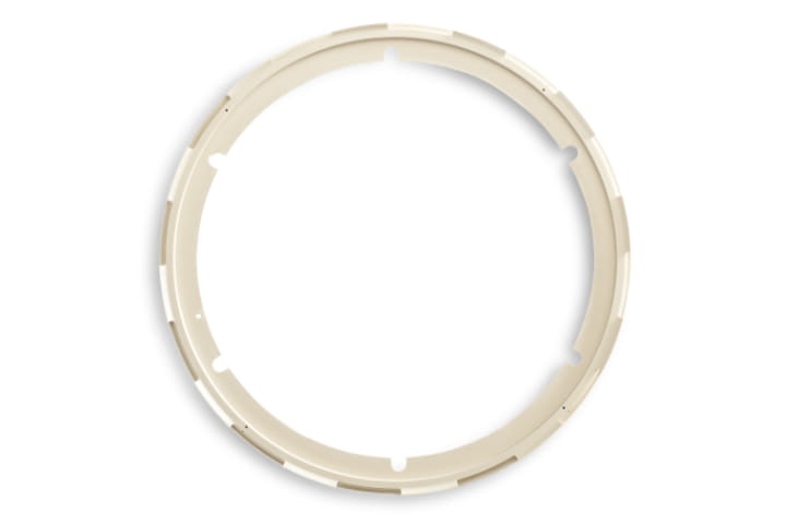
Wafer Clamp Ring
Semiconductor fabrication equipment relies on a vast range of different components made of high performance plastics. Among other parts, wafer rings or more precisely wafer clamp rings are commonly used for supporting and accurately positioning the wafer throughout various processing operations. Clamping the wafer is critical for maintaining precise processing tolerances, thus maintaining wafer yields.

Enabling accurate and clean wafer clamping
Components surrounding the wafer, such as clamp rings, need to withstand the stringent conditions and forces in the processing chambers. Depending on the processing conditions, the right material choice for the wafer clamp ring is essential for ensuring dimensional and mechanical stability, which directly impacts process performance and yield. Despite properties like mechanical strength, temperature resistance, chemical resistance, and in some cases, plasma resistance, the wafer ring material also needs to show high purity levels and low outgassing to minimize contamination and defects.
In wet processes, such as wet benches, single wafer cleaner, coater/developer or CMP, the components’ material requirements focus on chemical resistance, dimensional stability, purity, and strength. In most cases, the clamp rings are made of unfilled PEEK plastic, TECAPEEK SX natural or unfilled PPS plastic, TECATRON SX natural. PEEK is commonly used for parts exposed to higher temperatures and mechanical stresses, while PPS thermoplastic is the more economical alternative for parts with less stringent requirements. For clamp rings requiring more increased strength, PEEK CF30, TECAPEEK CF30 black is extensively used. For electrostatic discharge requirements, electrically conductive materials like TECAPEEK ELS nano black and TECAPEEK ELS CF30 black are chosen as clamp ring material.
The broadest portfolio for clamp ring materials

As a PPS supplier Ensinger’s unfilled PPS plastic sheets, TECATRON natural, have been developed specially for maintaining precise tolerances for critical parts like wafer clamp rings by reducing internal stresses to a minimum.
Moreover, the SX and ELS series are included in Ensinger's semiconductor grade portfolio, that is produced with stringent contamination controls and offering copy exact compliance. In this way, Ensinger ensures the highest level of cleanliness and quality performance consistency.
Reducing Ring Costs - find the best fitting size
With our PPS material TECATRON SX natural and PEEK material TECAPEEK SX natural Ensinger offers a wide range of tube dimensions for the semiconductor industries demands. In addition to a wide range of tube sizes in stock, custom order dimensions are available on request.
Wafer size |
06" (150 mm) |
08" (200 mm) |
12" (300 mm) |
|
Dimensions (OD / ID) |
||||
| 180 / 125 | 230 / 150 | 280 / 210 | 340 / 260 | |
| 180 / 130 | 230 / 180 | 285 / 180 |
340 / 310 | |
| 180 / 140 | 230 / 190 | 285 / 190 | 350 / 300 | |
| 180 / 150 | 230 / 195 | 285 / 195 | 360 / 290 | |
| 180 / 160 | 230 / 200 | 285 / 200 | 360 / 295 | |
| 185 / 125 | 238 / 210 | 285 / 210 |
364 / 260 | |
| 185 / 130 | 250 / 180 | 285 / 220 |
||
| 185 / 140 | 250 / 190 | 300 / 180 | ||
| 185 / 150 | 250 / 195 |
300 / 190 |
|
|
| 185 / 160 |
250 / 200 | 300 / 195 | ||
| 190 / 125 | 250 / 210 | 300 / 200 | ||
| 190 / 130 | 250 / 220 | 300 / 210 | ||
| 190 / 140 | 255 / 180 | 300 / 220 | ||
| 190 / 150 | 255 / 190 | 305 / 180 | ||
| 190 / 160 | 255 / 195 | 305 / 190 | ||
| 200 / 125 | 255 / 210 | 305 / 195 | ||
| 200 / 130 | 255 / 220 | 305 / 200 | ||
| 200 / 140 |
277 / 180 | 305 / 210 | ||
| 200 / 150 | 277 / 190 | 305 / 220 | ||
| 200 / 160 | 277 / 195 | |||
| 200 / 175 | 277 / 200 | |||
| 210 / 125 | 277 / 210 | |||
| 210 / 130 | 277 / 220 | |||
| 210 / 140 | 280 / 180 | |||
| 210 / 150 | 280 / 200 |


