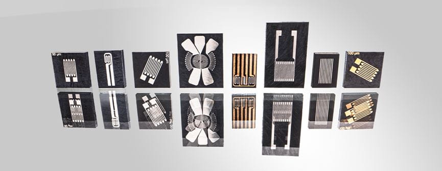
EMST Sensors: Revolutionising technology

Functionalisation, individualisation & integration – beyond common microsystems

Ensinger Microsystems Technologys (EMST) based sensor manufacturing solutions enable functionalisation, integration and individualisation of sensors through PEEK-based wafers and our newly developed technology, offering solutions beyond traditional options. With this, we are introducing a paradigm shift in sensor manufacturing. Our sensors based on high-performance plastic wafers provide an innovative, functionalisable, customisable and fully integratable alternative, replacing components with a new generation of sensors.

With local manufacturing, established supply chains and microsystems experts at every stage, we ensure the highest quality from the raw material to the finished sensor. Restrictions such as complex process chains, customisation options depending on the lot size or cleanroom constraints hinder creativity and innovation in sensor technology. Our solution frees sensors from unnecessary constraints, enabling a fresh perspective on manufacturing and fostering the development of new, innovative, cost-effective, customisable and sustainable solutions across industries worldwide.
Rethinking sensors with Ensinger Microsystems Technology

Sensor functionalisation

Ensinger Microsystems Technology (EMST) extends the possibilities of sensor production with tailor-made coatings that go beyond traditional options such as gold, nickel and copper. 

Sensor integration

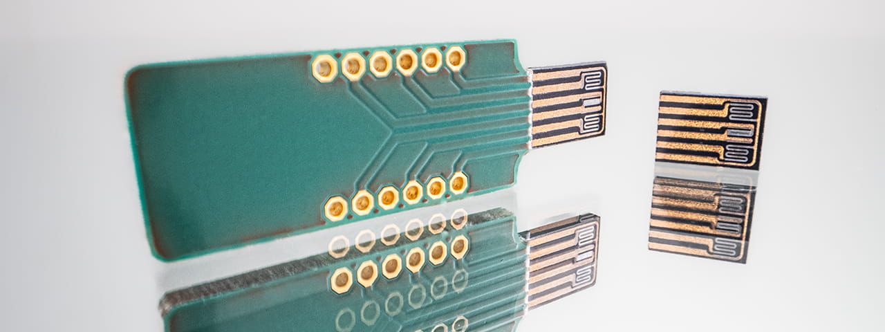
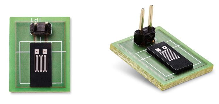
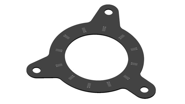
Our PEEK-based wafer allows versatile moulding for seamless integration into specific installations, promoting new possibilities efficiently and even in small quantities. With this, the sensor can be optimally adapted to the application.

Sensor individualisation

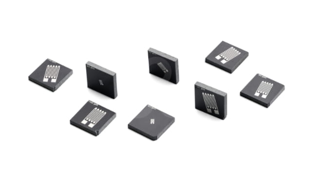
EMST takes customisation to new heights, enabling custom features, shapes, quantities and sizes never before possible. Achieve unprecedented levels of customisation to meet your specific needs.

Sensor product range and custom solutions 

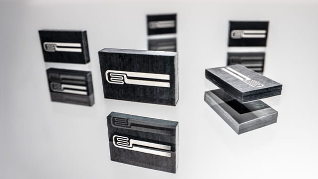
With in-house production and partnerships with the "Institut für Mikroproduktionstechnik der Leibniz Universität Hannover" (IMPT) and "Hahn Schickard Gesellschaft für angewandte Forschung e.V.", we provide limitless technical possibilities. By combining the advantageous properties of the high-performance plastic TECACOMP PEEK LDS with microsystems technology processes, functionalised, integrated and fully customisable sensors are created. 

Explore our diverse sensor solutions, including pressure, strain gauge, temperature, flow, and magnetic field sensors (AMR, GMR and eddy current).
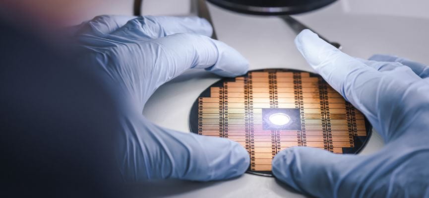

Revolutionising sensor solutions: Technological advantages with EMST sensors

Our high-performance plastic-based wafers address challenges such as heat, outgasing and chemical resistance, making them suitable for replacing silicon, glass or ceramic-based wafers. But our EMST takes sensor manufacturing one step further: by implementing thin-film structures that incorporate different metals or alloys for tailored functionality, we create functionalised sensors that can be fully integrated due to the ease of processing the material. Offering novel contact options on both sides, our easy-to-process materials ensure customised solutions. This allows us to create individual solutions for size, quantity, sensor placement, sensor number and more. With Ensinger Microsystems Technologies new approach, we manufacture existing components more easily and efficiently, or create completely new, integrated solutions.

Benefit from:
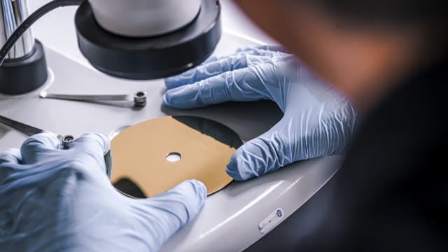
  • Streamlined and secure process chains over silicon-based alternatives
  • Customisable size, shape and quantities at reasonable cost
  • Functional layers as required
  • Secure supply chain
  • In-house development and manufacturing in Germany

PRODUCTION OF SENSOR SYSTEMS: EASIER, FASTER, CUSTOMISED - ALL FROM A SINGLE SOURCE

Conventional process chain on silicon & ceramics

New process chain on PEEK-based TECAWAFER

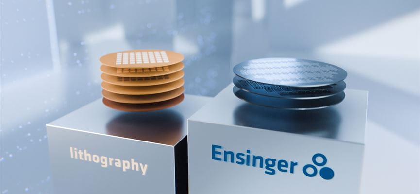
Conventional sensor systems are currently still structured using lithography processes. Due to the photo-resist-based structuring processes, the established production processes for sensor manufacturing must necessarily take place in a cleanroom environment, making high investments in infrastructure and plant operation necessary.
Our EMST manufacturing process uses plastic injection molding to produce substrates that can be manufactured in high volumes on a microstructured mold insert. Instead of structuring individual silicon, glass, sapphire and ceramic wafers or foil substrates, the number of individual process steps can be significantly reduced.

Ready to rethink sensor production?

Our current areas of application for EMST sensors include:

  • Pressure Sensors
  • Strain Gauges
  • Temperature Sensors
  • Current Sensors
  • Magnetic Field Sensors and more

We are also happy to advise you on the possibilities of sensors with EMST.
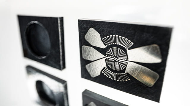

emst sensor case studies

Pressure sensor

made of TECACOMP PEEK LDS

A new approach to pressure sensor manufacturing from EMST

EMST introduces a new approach to pressure sensor manufacturing. By using PEEK-based wafers, we simplify production processes and eliminate complex procedures and harsh chemicals. Our innovative processes deliver pressure sensors with increased functionality and customisation. EMST specialises in fully integrated differential pressure sensors and offers unrivalled flexibility for customer-specific solutions.

Temperature sensor

made of TECACOMP PEEK LDS

Redefining temperature sensor manufacturing with EMST

EMST is redefining the way temperature sensors are made. Moving away from traditional materials, we are using TECACOMP PEEK LDS to unlock opportunities beyond conventional sensor manufacturing. With its lower thermal conductivity and versatile functionalisation capabilities, EMST offers solutions that are functional, integrable and customisable. Our substrate options meet a wide range of sensor requirements.

Flow sensor

made of TECACOMP PEEK LDS

Revolutionising flow sensor technology with EMST

EMST is at the forefront of transforming flow sensor manufacturing with our newly invented technology tailored for PEEK-based substrates. Our collaboration with Hahn Schickard has resulted in a thermal flow sensor that exploits the unique properties of our materials. This innovation opens the door to functional, integratable and fully customisable solutions, paving the way for new possibilities in sensor technology.